Explore
Featured
Recent
Articles
Topics
Login
Upload
Featured
Recent
Articles
Topics
Login
Upload
Search Results for 'Wafer-Swiss'
Wafer-Swiss published presentations and documents on DocSlides.
Improved Performance of 3DIC Implementations Through Inhere
by myesha-ticknor
Kwangsoo. Han, . Andrew B. Kahng. and Jiajia Li...
Brizon
by marina-yarberry
. Inc. www.brizon.net. y. uxinhu@brizon.net. Pro...
Load Lock Gun2 Status Update & (Revisionist?) History
by tawny-fly
Load lock gun worked very well in the Test Cave, ...
Directed Energy for Interstellar Flight
by debby-jeon
Philip Lubin. Physics Dept – UC Santa Barbara....
CORPORATE INSTITUTE OF SCIENCE & TECHNOLOGY , BHOPAL
by pasty-toler
DEPARTMENT OF ELECTRONICS & COMMUNICATIONS . ...
1 A. Macchiolo,
by faustina-dinatale
for the MPP, HLL, LAL, LPNHE, Glasgow, Liverpool...
Optimizing high frequency ultrasound cleaning in the semico
by pamella-moone
Steven Brems. Outline. Introduction to particle r...
I n the Christian tradition is a celebration commemorating
by ellena-manuel
Christmas. The most important and the most moving...
1 ICC Proprietary
by briana-ranney
MEMS DEVICE WAFER LEVEL PACKAGING. TECHNICAL PRES...
Impact of Wafer Backside Cu Contamination to
by yoshiko-marsland
18 um node Devices S Q Gu L Duong J Elmer S Prasad...
Fujitsu Microelectronics America Inc
by pamella-moone
Wafer bumping services are offered as a preparato...
www.technimex.com
by debby-jeon
Centric butter y valves, wafer, lugged and anged...
Combinations
by pasty-toler
Objectives:. I can predict and find the number of...
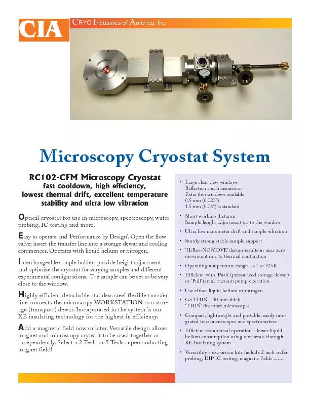
ciency, ptical cryostat for use in microscopy, spectroscopy, wafer pr
by alida-meadow
RYO Microscopy Cryostat System RYO Compact - l...
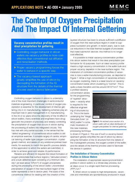
formanve for IG purposes. Suvh an ideal vavanvy profile means a high v
by natalia-silvester
vies is now a wafer-manufavturing provess, as depi...
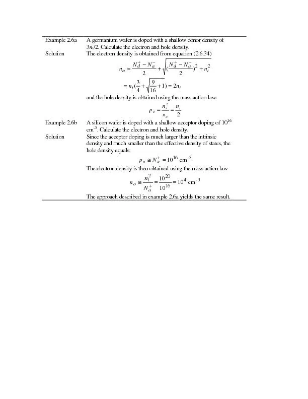
Example 2.6a A germanium wafer is doped with a shallow donor density o
by tatiana-dople
The electron density is obtained from equation (2....
MonolithIC 3D
by phoebe-click
. Inc. Patents Pending. 1. THE MONOLITHIC 3D-...
Techniques of Synthesizing
by test
Wafer-scale . Graphene. Zhaofu. ZHANG. 2022 2056...
ETCHING
by yoshiko-marsland
Università degli Studi di Roma “La Sapienza”...
Please contact offices below with your diamond wire, wafer grinding, a
by liane-varnes
NORTH AMERICA ASIA ASIA EUROPE Saint-Gobain Abrasi...
Dicing Advanced Materials for Microelectronics Annette Teng Cheung, Ph
by lindy-dunigan
B. Preparation of Bumped Wafer for Dicing Addition...
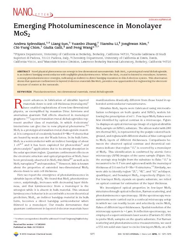
wafer.Inbothcases,thespectrawererecordedbyaspectrometerequippedwithali
by tatyana-admore
FIGURE1.ExfoliatedMoS akesonaSi/SiOsubstrate.(a)Op...
Robert Hsieh/Slide
by trish-goza
1. Technology Trends and Manufacturing Considerat...
1Dp230 at 5:1 dilution in TAE with 12.5mM MgCl2 - on eithe
by lois-ondreau
SiOn. as shown below. -apply 5ul 1dp230 10nM 1:5...
班 級
by alexa-scheidler
:. 應科二. 學 號 . :. . 9873622. �...
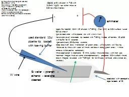
Microfabrication
by tawny-fly
of thin silicon cooling plates. 4” silicon waf...
Wafer Level Reliability
by natalia-silvester
2. Raw Material. Supplier. (i.e. Leadframe). Comp...
Low material budget
by natalia-silvester
microfabricated. cooling devices for particle de...
Wafer Edge ExclusionKevin Fisher
by ellena-manuel
OutlineMotivation for reducing edge exclusion
As discussed in Chapter 1, the industry
by yoshiko-marsland
Upgrading to a New Wafer SizeWafer size increases ...
Unpackaged Die and Wafer Storagehttp://www.national.com/en/die/appsnot
by celsa-spraggs
Proper storage conditions are necessary to prevent...
1 A. Macchiolo,
by trish-goza
for the MPP, HLL, LAL, LPNHE, Glasgow, Liverpool...
SEMICONDUCTOR DEVICE FABRICATION
by sherrill-nordquist
AN OVERVIEW. Presented to. EE 2212. Text Section ...
Load More...