PPT-Development of n-in-p large-area silicon microstrip sensors
Author : lois-ondreau | Published Date : 2016-04-25
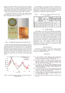
Y Unno for the ATLAS12 sensor community and Hamamatsu Photonics KK 201393 HSTD9 Y Unno 1 ATLAS Tracker Layouts Current inner tracker Pixels 512 cm Si area 27 m
Presentation Embed Code
Download Presentation
Download Presentation The PPT/PDF document "Development of n-in-p large-area silicon..." is the property of its rightful owner. Permission is granted to download and print the materials on this website for personal, non-commercial use only, and to display it on your personal computer provided you do not modify the materials and that you retain all copyright notices contained in the materials. By downloading content from our website, you accept the terms of this agreement.
Development of n-in-p large-area silicon microstrip sensors: Transcript
Download Document
Here is the link to download the presentation.
"Development of n-in-p large-area silicon microstrip sensors"The content belongs to its owner. You may download and print it for personal use, without modification, and keep all copyright notices. By downloading, you agree to these terms.
Related Documents