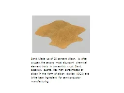
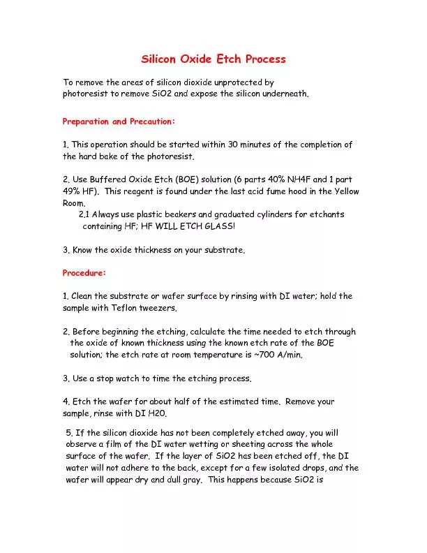
PDF-To remove the areas of silicon dioxide unprotected by expose the silic

Author : lindy-dunigan | Published Date : 2016-03-21

ich is hydrophobic Observe the backside of the wafer to confirm this effect for a few seconds removed immerse the substrate tion Etch for an additional 30 7 Repeat

Presentation Embed Code

Download Presentation

Download Presentation The PPT/PDF document "To remove the areas of silicon dioxide u..." is the property of its rightful owner. Permission is granted to download and print the materials on this website for personal, non-commercial use only, and to display it on your personal computer provided you do not modify the materials and that you retain all copyright notices contained in the materials. By downloading content from our website, you accept the terms of this agreement.

To remove the areas of silicon dioxide unprotected by expose the silic: Transcript


ich is hydrophobic Observe the backside of the wafer to confirm this effect for a few seconds removed immerse the substrate tion Etch for an additional 30 7 Repeat step 6 until SiO2 is. Preshower. for the CMS: BARC Participation . Anita . Topkar. BARC. CMS Preshower Detector. End caps of . CMS detector has ~4300 . silicon . strip detectors covering . area . of~17 . m. 2 . . BARC . Werner Bergholz, Jacobs University Bremen. Friedrich Passek, . Siltronic. AG. Peter Wagner. Updated . October 23, 2014. Task . Forces. . with. European . Participation. Int. . Advanced. Wafer . Geometry. After procuring raw sand and separating the silicon, the excess material is disposed of and the silicon is purified in multiple steps to finally reach semiconductor manufacturing quality which is called electronic grade silicon. The resulting purity is so great that electronic grade silicon may only have one alien atom for every one billion silicon atoms. After the purification process, the silicon enters the melting phase. In this picture you can see how one big crystal is grown from the purified silicon melt. The resulting mono-crystal is called an ingot.. Localisation. using. MAX-SAT & Backbones. Georg Weissenbacher. Charlie . Shucheng. Zhu, . Sharad. . Malik. Princeton University. (Photo: Intel Press Kit). Where did things go wrong?. Intel Pentium FDIV Bug 1994. Hrvoje Štefančić. . Theoretical Physics Division . Ruđer Bošković Institute . (based on joint work with . Hrvoje Abraham . and . Predrag Lazić. ). Electric field strength in a segment of a Si microstrip detector. Hafezi. , S. Mittal, J. Fan, A. . Migdall. , J.M. Taylor, Nature Photonics, . (. 2013. ) . doi:10.1038/nphoton.2013.274. . Topology . -- the understanding of how things are connected -- remains abstract, even with the popular example of doughnuts and coffee cups. This concept, esoteric as it appears, is also neat because it is the basis for creating . Swaroop K. Behera. 1. , . Shvetashwa. Suri. 1. Pradeep Rohatgi. 1. , Nathan Salowitz. 2. 1. Department of Material Science and Engineering, UW-Milwaukee . 2. Department of Mechanical Engineering , UW-Milwaukee. - Frederick Douglass. Frederick Douglass. “I expose slavery in this country, because to expose it is to kill it. Slavery is one of those monsters of darkness to whom the light of truth is death.” . it—Part 1. Explain . how single crystalline Si wafers are made . Describe . the crystalline structure of Si . Find . the . Miller indices. of a planes and directions in crystals and give the most important direction/planes in silicon . Titanium Dioxide Market report provides the future growth trend of the market based on in-depth research by industry experts.The global and regional market share along with market drivers and restraints are covered in the report. View More @ https://www.valuemarketresearch.com/report/titanium-dioxide-market Jordan . Radice. jordanra@buffalo.edu. Advanced . VLSI. Spring 2015. Dr. Ram Sridhar. Background. Moore’s Law (As we all know): Doubling of transistors every 1.5 ~ 2.0 years.. Dennard scaling works in conjunction with Moore’s law in that we maintain the overall power density of the chip area despite the exponential increase in transistors.. O ttawa PublicHealth .ca | SantePubliqueO ttawa.ca 613 - 234 - 4641 | TTY/ATS : 613 - 580 - 9656 EMERGENCY CONTRACEPTION What is emergency contraception? Emergency contraception consists of m eth Obtain the PDF of Moles, Warts & Skin Tags Removal™ eBook authored by Charles Davidson – a comprehensive digital program designed to help you naturally eliminate moles, warts, & skin tags within three days without resorting to surgery. Foot warts are a type of warts that can be found at the bottom of the foot. A foot wart is about 1cm in diameter and is generally paler than the nearby skin. It has tiny black dots at the centre.

Download Document

Here is the link to download the presentation.
"To remove the areas of silicon dioxide unprotected by expose the silic"The content belongs to its owner. You may download and print it for personal use, without modification, and keep all copyright notices. By downloading, you agree to these terms.

Related Documents